

Day 8 Entrep Community
Hello, welcome!
GUIDELINES
Be helpful and relevant
This community is intended to provide helpful,... View more
Organizer:
- Organized by
-
-
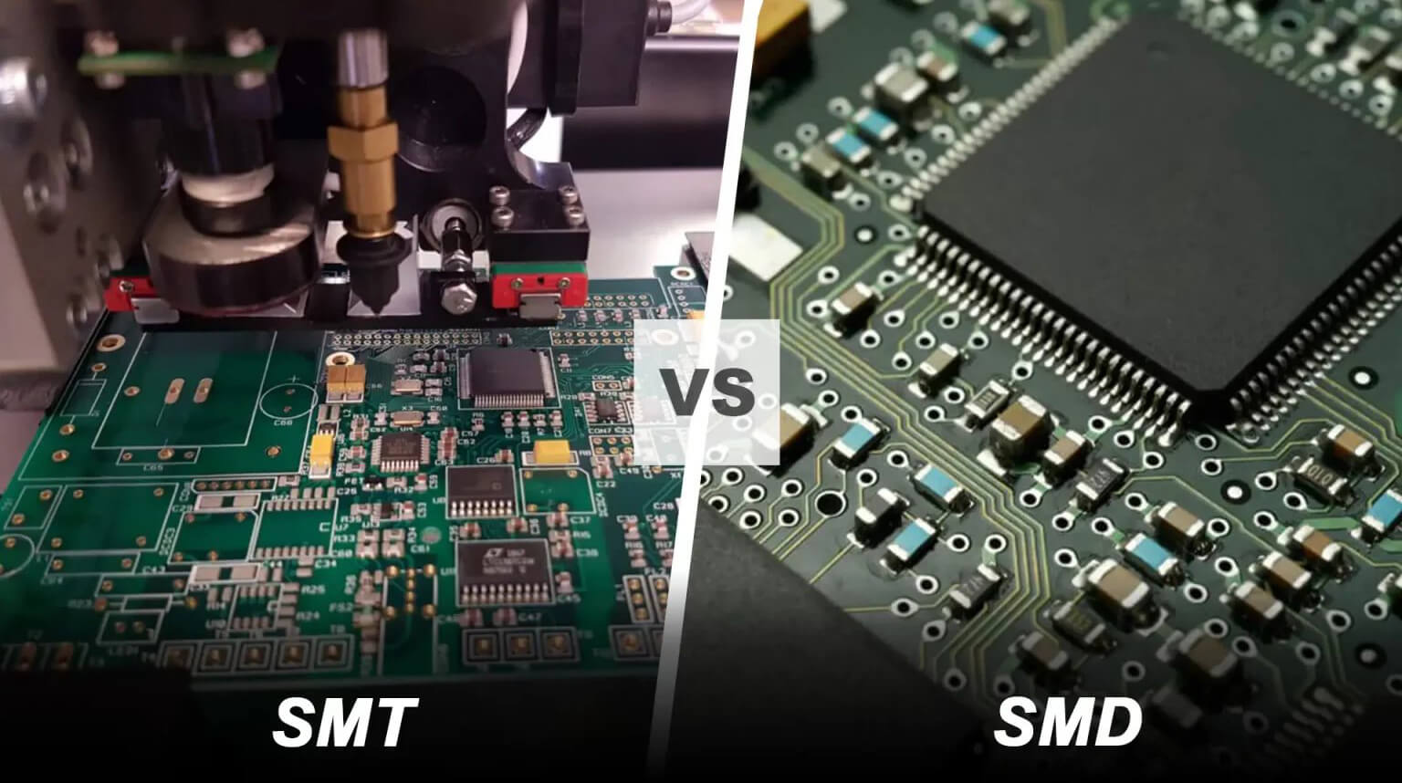
High-Density Electronic Assembly Techniques in Modern PCB Manufacturing
-
High-Density Electronic Assembly Techniques in Modern PCB Manufacturing
The electronics industry is evolving rapidly, with continuous demand for smaller, faster, and more efficient devices. To meet these requirements, manufacturers rely on highly precise and automated PCB assembly techniques that can support complex and compact circuit designs. In this context, understanding SMT vs SMD is essential because these concepts are directly related to how modern electronic components are designed, placed, and assembled on printed circuit boards.
As electronic systems become more advanced, traditional assembly methods are no longer sufficient to handle high-density layouts and mass production requirements. This has led to the widespread adoption of surface-based manufacturing processes that improve accuracy, efficiency, and scalability in modern electronics production.
Development of PCB Assembly Technology
In earlier stages of electronics manufacturing, through-hole assembly was commonly used. This method required component leads to pass through drilled holes on the PCB and be soldered on the opposite side. While it provided strong mechanical strength, it limited circuit density and slowed down production.
With the growing need for compact and high-performance electronic devices, manufacturers shifted toward surface-based assembly methods. Instead of inserting components through holes, parts are now placed directly onto the PCB surface. This change allowed for higher component density, faster production cycles, and more flexible circuit designs.
Today, surface-based assembly is the standard approach in most modern electronic products.
Working Process of Surface-Mount Assembly
Surface-mount assembly is a fully automated process designed for fast and accurate PCB manufacturing. It removes the need for drilling holes for most components, simplifying both design and production.
The process begins with the application of solder paste onto PCB pads using a precision stencil. After that, automated pick-and-place machines position electronic components onto the board with high accuracy. The PCB then passes through a reflow oven, where controlled heat melts the solder and forms permanent electrical connections.
This highly efficient process enables large-scale production of complex circuit boards while maintaining consistent quality.
Features of Surface-Mounted Components
Surface-mounted components are specifically designed for direct placement on PCB surfaces. They are smaller, lighter, and more compact compared to traditional through-hole components.
Their reduced size allows engineers to design high-density circuits that occupy less space while maintaining strong performance. Since they do not require drilled holes, PCB layout becomes more flexible and efficient.
These components include resistors, capacitors, diodes, transistors, integrated circuits, and connectors, all optimized for modern electronic applications.
Key Benefits of Surface-Based Assembly
One of the biggest advantages of surface-based assembly is automation. Advanced machines can place thousands of components per hour with high precision, significantly reducing human error and improving production speed.
Another major benefit is miniaturization. Components mounted directly on the PCB surface allow for smaller and lighter electronic products, which is essential for devices like smartphones, wearables, and portable gadgets.
Electrical performance is also improved because shorter signal paths reduce resistance, inductance, and noise. In addition, eliminating most drilled holes supports more efficient multilayer PCB designs.
Cost efficiency is another important advantage, as automated production reduces labor requirements and supports high-volume manufacturing.
Comparison with Through-Hole Assembly
Through-hole and surface-based assembly methods differ in structure and application. Through-hole assembly involves inserting component leads into drilled holes, while surface-based assembly mounts components directly onto PCB pads.
Through-hole technology provides strong mechanical support and is suitable for heavy components or high-vibration environments. However, it requires more space and reduces design flexibility.
Surface-based assembly offers higher density, faster production, and better compatibility with automated systems. Due to these advantages, it has become the dominant method in modern electronics manufacturing.
In some designs, both methods are combined to meet specific mechanical and electrical requirements.
Importance of Precision in PCB Assembly
Precision is critical in PCB manufacturing because even minor errors can impact circuit performance. Modern systems use advanced robotics and optical inspection tools to ensure accurate component placement.
Solder paste must be applied carefully to avoid defects such as bridging or weak joints. Reflow temperature control is also essential to ensure proper solder formation without damaging components.
Inspection techniques like automated optical inspection and X-ray analysis help detect manufacturing defects early, ensuring high product quality.
Challenges in Surface-Mount Manufacturing
Despite its advantages, surface-mount assembly also comes with challenges. Thermal stress during soldering can damage sensitive components if not properly controlled.
Miniaturization makes inspection and repair more difficult, requiring advanced tools and strict manufacturing environments. High-speed production may also lead to alignment errors that affect performance.
Some components are also moisture-sensitive and require careful handling and storage to avoid damage during assembly.
PCB Design Considerations for Manufacturing
Good PCB design is essential for smooth manufacturing. Proper spacing between components ensures easier soldering and inspection while reducing interference.
Pad design must be carefully optimized because incorrect sizing can lead to poor solder joints. Thermal management is also important for components that generate heat during operation.
Proper grounding, routing strategies, and layer planning help improve signal integrity and reduce electromagnetic interference. Clear documentation and labeling further support efficient production.
Close collaboration between designers and manufacturers helps prevent issues early in the development process.
Quality Control in Electronics Production
Quality control plays a major role in ensuring reliable electronic products. Multiple inspection methods are used throughout the manufacturing process.
Automated optical inspection detects placement and alignment issues, while X-ray systems identify hidden solder joint defects. Functional testing ensures that circuits operate correctly under real-world conditions.
Environmental testing such as thermal cycling and vibration testing is used to evaluate long-term durability and reliability.
These steps ensure that only fully tested and high-quality products reach the market.
Industrial Applications of Modern PCB Assembly
Modern PCB assembly techniques are widely used across many industries. Consumer electronics rely on compact surface-mounted designs for smartphones, laptops, tablets, and wearable devices.
In automotive systems, these methods are used for control units, sensors, and communication modules. Medical equipment also depends on reliable compact electronics for monitoring and diagnostic devices.
Industrial automation, aerospace systems, and telecommunications infrastructure all benefit from high-density PCB designs and advanced manufacturing techniques.
Future of PCB Assembly Technology
The future of PCB manufacturing is moving toward greater automation, intelligence, and miniaturization. Artificial intelligence is increasingly being used to improve production efficiency and defect detection.
Flexible and rigid-flex PCBs are becoming more common as devices become thinner and more adaptable. Advanced packaging technologies are enabling higher performance in smaller spaces.
Sustainable manufacturing practices are also gaining importance, focusing on reducing waste and improving energy efficiency.
Conclusion
Modern PCB assembly technologies have significantly transformed electronics manufacturing by enabling compact, efficient, and highly reliable circuit production. Automated processes, precise component placement, and advanced inspection systems ensure consistent quality in large-scale production.
Understanding these assembly techniques is essential for engineers and designers working in electronics. With proper design strategies and strict quality control, modern manufacturing methods continue to drive innovation across the entire electronics industry.

pcbcool.com
SMT vs SMD: What’s the Difference in PCB Assembly? | PCBCool
Learn the difference between SMT and SMD in PCB assembly. A beginner-friendly guide explaining definitions, key differences, and how they work together in electronics manufacturing.
Log in to reply.